Wikimedi'Òc
Modes d'emploi

Cet album fait partie des albums
Cet album photos contient les sous-albums suivants :


Microprocessore silicio germano.jpg - Djdomix~commonswiki

OR2 layout.PNG - Paintman

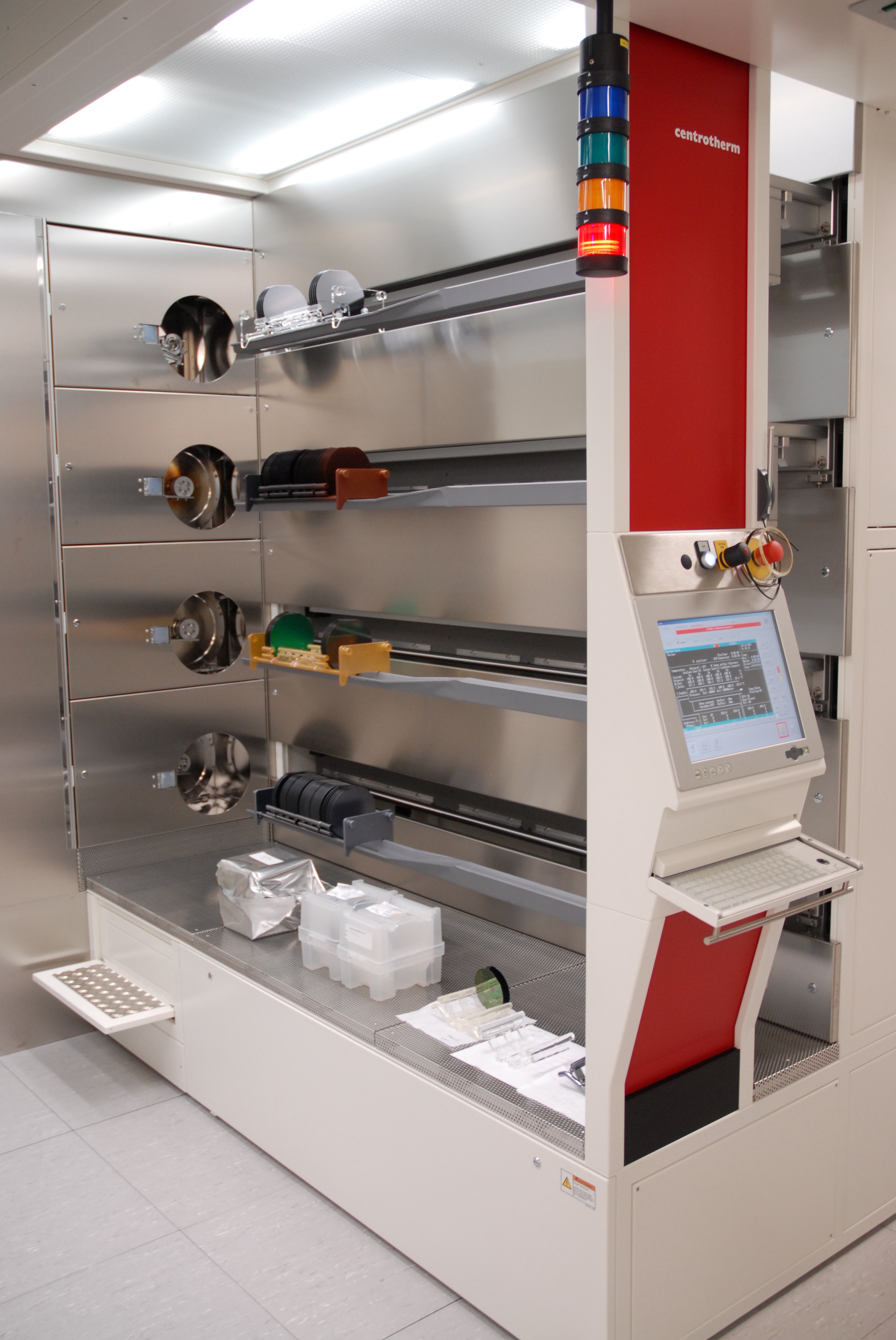
Centrotherm diffusion furnace at LAAS 0489.jpg - Guillom

Centrotherm diffusion furnace at LAAS 0491.jpg - Guillom
Centrotherm diffusion furnace at LAAS 0493.jpg - Guillom
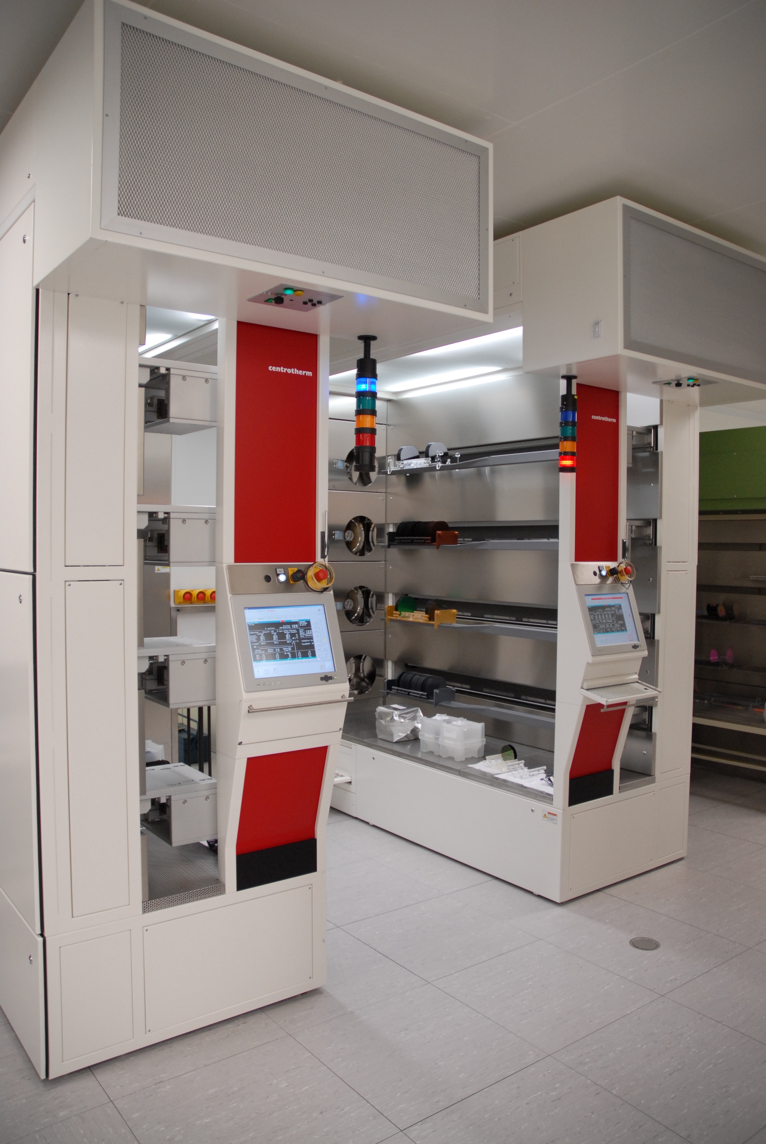
Centrotherm diffusion furnaces at LAAS 0481.jpg - Guillom

Lift-off (microtechnology) process.svg - Cepheiden
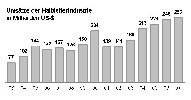
Worldwide Semiconductor Sales in Billion US-Dollar GERMAN.jpg - Swettengl
APD.png - Mehanik

Alu bridge.jpg - PhysikingerC
Organic transistor Greek.png - Drxai
Siliconchip by shapeshifter.png - Tothwolf

Illustration of C-V measurement.gif - Beatnik8983

Lift-off-Verfahren (Halbleitertechnik).svg - Cepheiden
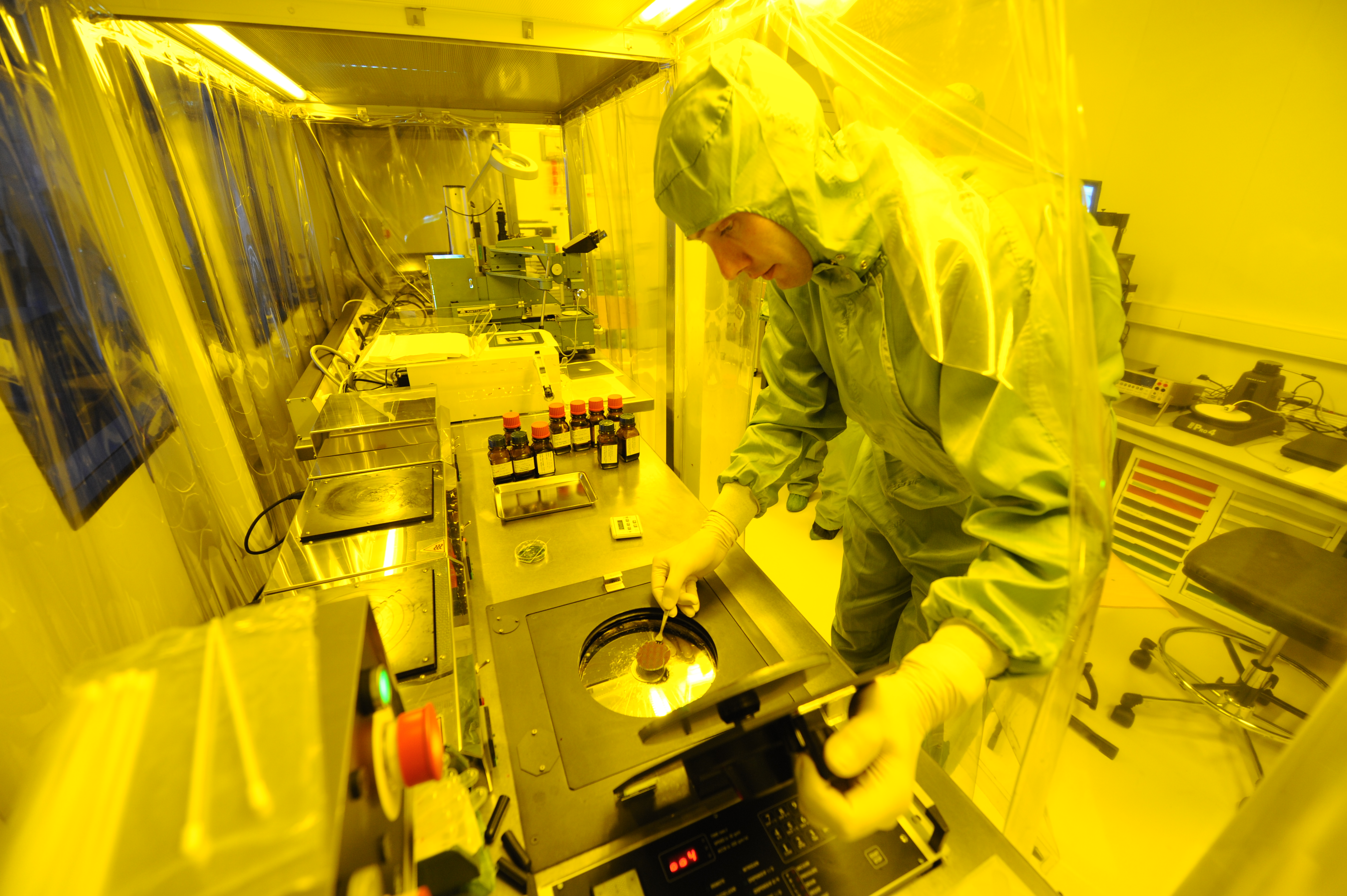
Salle blanche ensim.jpg - Clem-ensim
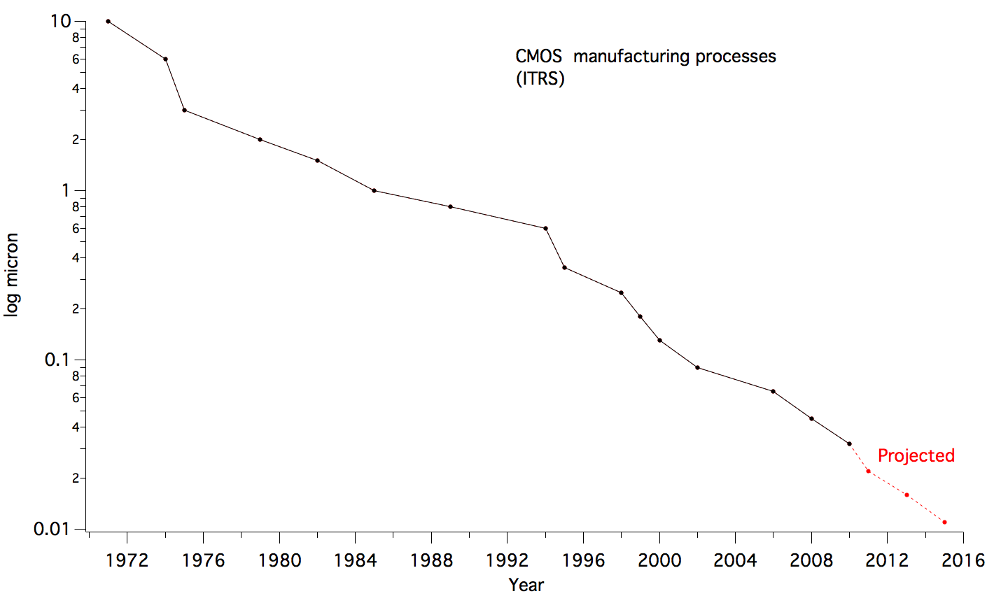
SemiconductorProcessSize.png - Bazorg
Schottky-Transistor-Side.svg - Mikhail Ryazanov

Comparison semiconductor process nodes.svg - Cmglee
Spacer Patterning.JPG - File Upload Bot (Magnus Manske)
Spacer formation (DE).svg - Cepheiden

Lift-off-Verfahren (Fehlerbilder).svg - Cepheiden

4-fach-NAND-C10.JPG - Dgarte

Buried zener vs npn epi.svg - Retired electrician

Buried zener structure.svg - Retired electrician

GST CVD setup.png - Sebastian Wallroth

GeS CVD setup.png - NovelGlass
GST CVD setup.tif - NovelGlass

Overlay - typical model terms DE.svg - Cepheiden
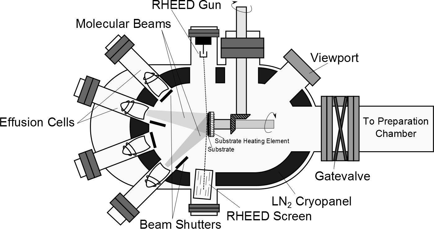
Molecular Beam Epitaxy.png - Pnikhil~commonswiki

Wafermap showing fully and partially patterned dies.svg - Moxfyre

14 nm half-pitch multipatterning.png - Chess

14 nm half-pitch multipatterning.svg - Chess
Bivar-logo.png - Bivar, Inc.

Bell telephone magazine (1922) (14569544079).jpg - Fæ
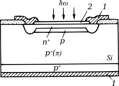
1957(Figure 9)-Gate oxide transistor by Frosch and Derrick.png - Wikain

Diferencia estructura.PNG - Cabenito

Framework for big data and analytics for semiconductors manufacturing.jpg - Ismat.marouf
Laser diode with case cut away.jpg - Arconsoli

7 nm litho options.png - FastilyClone
Anti-spacer Double patterning.png - FastilyClone
Spacer trimming.png - Guiding light

SADP then SATP.png - Guiding light

DRAM trench structure configuration1 1.svg - OgreBot

DRAM burried capacitor configuration.svg - FastilyClone

DRAM trench configuration 2.svg - FastilyClone

DRAM trench structure configuration1.svg - FastilyClone

Trilogy WSI Wafer.png - Richfiles

Ballbond-trand.png - Hshekhani

Overflow.svg - Menner

Self-aligned silicidation.svg - IohLai4cEx1be2biRee

SE Making Ingot Step 03.svg - JackPotte

SE Making Ingot Step 02.svg - JackPotte

SE Making Ingot Step 04 ver01.svg - JackPotte

Moore Kosten.png - Frank Klemm

10nm node mt1 ppe vs pitch.png - Willy1018

Field-induced MRAM schematic ja.png - Onosaki

Buried zener structure-en.svg - Zabacad

SADP challenge.png - Dave louis john

Line cut location offset.png - OgreBot

Two-bar challenge.png - Guiding light

APD structure.svg - Д.Ильин

APD with Superlattice.svg - Д.Ильин

LELE challenge.png - Hippymoose17

KO fig21 applications Corelv11.png - Jrvanommen
DRAM self-aligned storage node locations.png - Guiding light

Main applications of ALD.png - Jrvanommen

Piranha solution.png - Galaktico

The entrance of 3S Silicon Tech., Inc.jpg - 創造未來,迎接康莊

Dicing blade.jpg - Ja>HokuhokuhokukunOiso

Pellicle vs no pellicle in a photomask.svg - Thelichprince